Added nRF24 firmware and documentation
2 files modified
2 files added
| | |
|---|
| | | \end{figure} |
|---|
| | | |
|---|
| | | |
|---|
| | | \subsection{Connecting nRF24l01+} |
|---|
| | | |
|---|
| | | For fast communication Nordic Semiconductor chip nRF24l01+ is used. It operates on 2.4 GHz frequency band, supports multiple channels, raw communication with possibilities of ACK/NoACK. The delay of wirelessly transporting the trigger should be minimal with pair of nRF24 where one is designated as transmitter and one as receiver. There is possibility of full duplex communication. No protocol is defined yet, so we have multiple possibilities on implementation. |
|---|
| | | |
|---|
| | | As an advenced feature of the receiving end, there is a posibility to measure round trip of data transfer, therefore, the receiver can calculate the delay caused by the transmission and compensate for it, if the receiver does not need to trigger the event. As an example, this could be implemented when accelerometer is read and should be synchronized with camera frame capture. The receiver can measure acceleration beforehand in short intervals and put it into cyclic buffer. When the trigger is received and knowing the trigger transmission delay and accelerometer reading frequency, we can look up the value for acceleration at the exact time the camera published the event at the transmitter side. With this, we have possibility to minimize trigger delay. |
|---|
| | | |
|---|
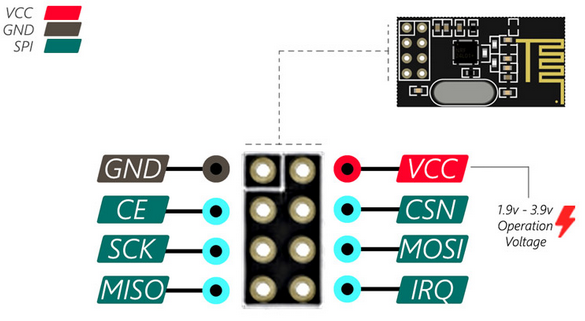
| | | nRF24l01 modules are used, where everyting regarding radio is implemented. Module has SPI and power supply pins on its connector. Image of module with its pinout is presented in figure \ref{fig:nrfpinout}. |
|---|
| | | |
|---|
| | | \begin{figure}[htb] |
|---|
| | | \begin{center} |
|---|
| | | \begin{minipage}{0.45\linewidth} |
|---|
| | | \includegraphics[width=0.9\linewidth]{figures/nrf_pinout.png} |
|---|
| | | \end{minipage} |
|---|
| | | \begin{minipage}{0.45\linewidth} |
|---|
| | | \includegraphics[width=0.9\linewidth]{figures/nrf_electrical.png} |
|---|
| | | |
|---|
| | | \end{minipage} |
|---|
| | | \end{center} |
|---|
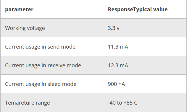
| | | \caption{nRF24l01 module pinout and its electrical characteristics. \cite{nrfInterfacing}}\label{fig:nrfpinout} |
|---|
| | | \end{figure} |
|---|
| | | |
|---|
| | | |
|---|
| | | |
|---|
| | | Connection to ESP32 module is as presented in the following table: |
|---|
| | | |
|---|
| | | \begin{tabular}{l | l | l} |
|---|
| | | nRF pin & ESP32 pin & comment \\ \hline |
|---|
| | | 1 & GND & Power and signal ground \\ |
|---|
| | | 2 & 3.3V & Power supply \\ |
|---|
| | | 3 & 22 & CE (Chip enable) \\ |
|---|
| | | 4 & 21 & CSN \\ |
|---|
| | | 5 & 18 & SCK \\ |
|---|
| | | 6 & 23 & MOSI \\ |
|---|
| | | 7 & 19 & MISO \\ \hline |
|---|
| | | \end{tabular} |
|---|
| | | |
|---|
| | | |
|---|
| | | |
|---|
| | | \section{Firmware} |
|---|
| | | |
|---|
| | | \subsection{Energy conservation} |
|---|
| | |
|---|
| | | /* There was a help from these two pages: |
|---|
| | | https://forum.arduino.cc/t/connect-nrf24l01-to-esp32/678710/4 |
|---|
| | | https://electropeak.com/learn/wireless-communication-w-arduino-and-nrf24l01/ |
|---|
| | | */ |
|---|
| | | |
|---|
| | | #include <RF24_config.h> |
|---|
| | | #include <nRF24L01.h> |
|---|
| | | #include <RF24.h> |
|---|
| | | #include <printf.h> |
|---|
| | | |
|---|
| | | #include<WiFi.h> |
|---|
| | | |
|---|
| | | #define IN_TRIGGER 18 |
|---|
| | | #define OUT_TRIGGER 19 |
|---|
| | | #define IN_TRIGGER 17 |
|---|
| | | #define OUT_TRIGGER 16 |
|---|
| | | |
|---|
| | | |
|---|
| | | RF24 radio(22, 21); // CE, CSN |
|---|
| | | |
|---|
| | | const byte address[6] = {'R','E','C','V', '1'}; |
|---|
| | | char dataToSend[4] = "TRG"; |
|---|
| | | |
|---|
| | | void IRAM_ATTR isr() { |
|---|
| | | digitalWrite(OUT_TRIGGER, HIGH); |
|---|
| | | radio.write( &dataToSend, sizeof(dataToSend) ); |
|---|
| | | delay(1); |
|---|
| | | digitalWrite(OUT_TRIGGER,LOW); |
|---|
| | | } |
|---|
| | | |
|---|
| | | |
|---|
| | | |
|---|
| | | void setup() { |
|---|
| | | // put your setup code here, to run once: |
|---|
| | |
|---|
| | | WiFi.mode(WIFI_OFF); |
|---|
| | | btStop(); |
|---|
| | | |
|---|
| | | |
|---|
| | | radio.begin(); |
|---|
| | | radio.openWritingPipe(address); |
|---|
| | | radio.setPALevel(RF24_PA_MIN); |
|---|
| | | //radio.setDataRate( RF24_250KBPS ); |
|---|
| | | |
|---|
| | | pinMode(IN_TRIGGER, INPUT_PULLUP); |
|---|
| | | pinMode(OUT_TRIGGER, OUTPUT); |
|---|
| | | attachInterrupt(IN_TRIGGER, isr, RISING); |
|---|
| | | |
|---|
| | | |
|---|
| | | } |
|---|
| | | |
|---|
| | | void loop() { |
|---|

